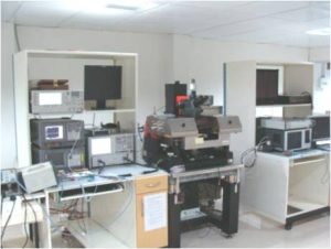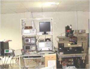


Test and Measurement
Techniques for operating test equipment and the relevant measurements that can be made at a high frequencies are covered by topics in this track. Equally important is knowledge of the inherent limitations of certain tests related to RF and Wireless performance.
This topic explains essential RF measurements that must be made on modern wireless communications equipment. The newest models of the necessary RF test equipment are explained and demonstrated, including vector network analyzers, spectrum analyzers, digitally modulated signal generators and vector signal analyzers.
RF Measurements:Principles & Demonstration
Course 11
Summary
This lecture-based course explains essential RF measurements that must be made on modern wireless communications equipment – mobile/smart phones, wireless LANs, GPS navigation systems, and others. Current models of the essential test instruments will be explained and demonstrated, including vector network analyzers, power meters, spectrum analyzers, digitally modulated signal generators and vector signal analyzers.
All of the measurements will be demonstrated on actual RF wireless components including power amps, LNAs, mixers, upconverters, and filters. These measurements will include traditional tests of power, gain, group delay, S parameters, AM to PM, intermodulation products, harmonics and noise figure. The unique measurements of wireless communications will then be made with PSK and FSK digitally modulated signals including spectral regrowth, constellation diagram distortion, error vector magnitude (EVM), and bit error rate.
Learning objectives
Upon completing the course you will be able to:
- describe the RF measurements that must be made on modern wireless communication equipment.
- take proper care of RF cables and connectors in the lab
- explain why the various measurements must be made.
- operate the RF test equipment that is used to make these measurements
- setup and calibrate a Vector Network Analyzer measurement
- make measurements on power amps, LNA’s, mixers, upconverters and filters
- make traditional tests of power, gain, group delay, S parameters, AM to PM, intermodulation products, harmonics, and noise figure with CW signals.
- ensure that distortion products from the instrumentation are not corrupting the measurement results
- develop reasonable expectations for measurement uncertainties.
Target Audience
Design and production engineers and technicians interested in improving measurement skills through a practical approach will benefit from this course. The lecture includes a review of wireless communication systems, RF components and the tests that must be made, making this an ideal course for professionals wishing to have a thorough grounding in the knowledge of how wireless systems operate.
Outline
Day One
Course Objectives and Course Outline
• Review of RF principles • Wave parameters – frequency, amplitude, phase • basics of propagation • dB and dBm • Mismatches • Conversion between mismatch expressions – Reflection coefficient, return loss, mismatch loss, SWR • The Smith Chart – an overview • S-parameters
RF Test Equipment – Principles of Operation
• Cable and connector types/proper care • Signal generators • Power meters and power sensors • Frequency counter • Vector network analyzer • Demonstration: how to setup and calibrate a basic VNA measurement • Vector network analyzer measurements on non-packaged devices
Day Two
• Spectrum analyzer • Demonstration: how to operate a spectrum analyzer – Resolution Bandwidth, Video Bandwidth, Attenuation, Scaling • Noise figure meter • Vector signal analyzer
Measurement Uncertainties
• Mismatch uncertainty • VNA – motivation for measurement calibration
RF Communication system block diagram
• Specifications of components to be tested
Transmitter components
Phase locked oscillator
• principles of operation • measurement of phase noise – log/video vs. rms averaging on Spectrum Analyzer – Marker noise function
Upconverter
• Modulation basics • principles of operation • demonstration: measurement of conversion gain using a spectrum analyzer – output spectrum of upconverter
Day Three
Power Amplifier
• principles of operation • demonstration measurement – swept gain – power sweep/1 dB compression point – AM to PM distortion – phase on the Vector Network Analyzer • Harmonic power using Spectrum Analyzer • checking for distortion products in the test equipment
Receiver Components
Noise and Noise Figure
• Noise figure measurement • demonstration measurement using Y-factor technique
Filters
• Principles of operation • Demonstration measurement – passband – inband loss – match – group delay on the Vector Network Analyzer
Day Four
Low Noise Amplifiers
• principles of operation • Noise figure • intermodulation products • demonstration measurement – gain/1dB compression point – output power – phase using power sweep on Vector Network Analyzer • demonstration measurement – S-parameters vs. frequency on the Vector Network Analyzer
Mixer
• principles of operation – conversion gain – output power
Intermodulation Products
• description of intermodulation products • Demonstration: IP3/TOI using a spectrum analyzer • definition of IP2
Overall Receiver Performance
• Typical overall receiver performance • Calculating system performance
Day Five
Multiple Access Techniques
• FDMA • TDMA • CDMA • OFDMA
Performance of RF components with digital signals
• Block diagram • Digital modulation fundamentals • demonstration measurement – Adjacent Channel Power (ACP) performance vs. power amplifier nonlinearity with different modulation techniques • zero span function on Spectrum Analyzer
Vector Signal Analyzer Modulation Quality Measurements
• Principles of operation • EVM/Distortion of digital signal due to power amplifier nonlinearity • EVM/Distortion of digital signal due to IF filter group delay • EVM/Distortion due to LO phase noise with mixer • Troubleshooting digital modulation with a Vector Signal Analyzer
Description of Bit Error Rate (BER)
Review
• RF Communication System Operation
I am item content. Click edit button to change this text. Lorem ipsum dolor sit amet, consectetur adipiscing elit. Ut elit tellus, luctus nec ullamcorper mattis, pulvinar dapibus leo.
These courses provide participants with theories, examples, and practical techniques for accurately modeling RF circuit components with modern CAE tools.
RF Fundamentals, Modeling and De-Embedding Techniques
Course 13
Summary
This 3-day course provides technical professionals with the fundamental concepts and engineering tools needed to understand RF fundamentals and test fixture de-embedding techniques. The latest software simulation tools are used to demonstrate these concepts and techniques.
Learning objectives
Upon completing the course you will be able to:
- Describe RF waves and their characteristics
- Understand how to model RF Passive devices and Test fixtures at RF Frequencies
- Understand Basic De-embedding Techniques
- Explain RF measurement & Calibration Techniques
- Understand Measurement Limitations and Error Functions
Target Audience
Test and measurement technicians and engineers who need to understand proper techniques for modeling fixtures and passive devices.
Outline
Day One
RF Fundamentals
• Characteristics of Electromagnetic Energy • Conductors vs. Transmission Lines • Voltage/Current Relationships • Complex Impedance and Admittance Systems • RF Transmission Lines • Impedance Transformations and Matching
The Smith Chart/Scattering Parameters
• Understanding the Fundamentals of the Smith Chart • Two-Port Definitions (S-parameters) • The 2*2 Scattering Matrix • Cascaded Two- Port Connections
Day Two
Passive Component Modeling
• Resistors at RF Frequencies • Straight Wire Inductance • Capacitors and Equivalent Models • Simulation Models Vs Measured Results • Package Parasitic Models
Transmission Lines and Ground Parasitics
• Via-Hole and Wrap Around Ground Inductance • Transmission Lines Analysis • Microstrip Line Modeling Vs Frequency • PCB Multilayer Designs and Tradeoffs, Ground Effects
Day Three
Measurements
• De-Embedding • De-Embedding Techniques (LRL,TRL, etc.) • Developing De-Embedding Test Fixture Models • Calibration and Measurement Error Corrections • Calculating Total Uncertainties • De-Embedding Using T-Parameters
